Products
Toys
Schools
Industry and Universities
ft Design Studio
Service
fischerTiP
Search for...
Home
Schools
Learning material
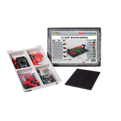
STEM Electronics
Learning material
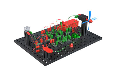
STEM Electronics
Get to know the extensive world of electronics
More information about STEM Electronics
Lesson plans STEM Electronics
Topic Introduction
Definition
History
Fundamentals
cd-84f54cbff4-7bk7r